
Infrastructure
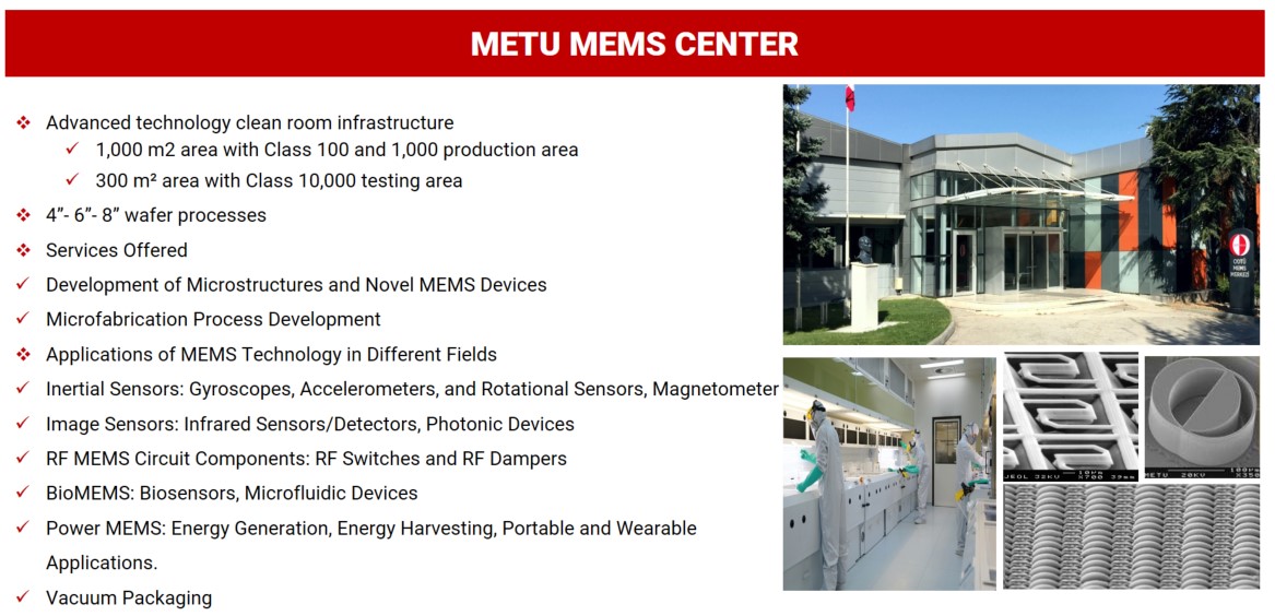
The center operates within a facility spanning a total of 4,500 m2, housing various cleanrooms of 100, 1,000, and 10,000 classes, as well as laboratories, seminar rooms, meeting areas, and offices. The center is located within the METU Technopark MET campus, managed by METU Technopark, and holds the status of a Technology Development Zone approved by the Ministry of Industry and Technology. The center, as well as the technopark companies, are situated within this campus. The METU MEMS Center features a dedicated cleanroom space of 1,300 m2 for carrying out MEMS fabrication.
MEMS fabrication processes are categorized based on the nature of the operation. These categories include Coating, High-Temperature Oxidation and Diffusion, Dry Deposition and Etching in a Plasma Environment, Lithography, Chemical Wet Etching and Cleaning, Measurement, Inspection & Testing, and Electronic Packaging and Integration.
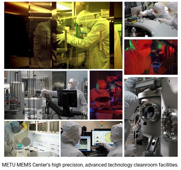
MEMS manufacturing techniques require the use of specialized equipment and devices. The cleanroom at METU MEMS Center is equipped with machinery and tools worth a total of 40 million US Dollars, financed through research projects following the initial infrastructure created by TESTAŞ.
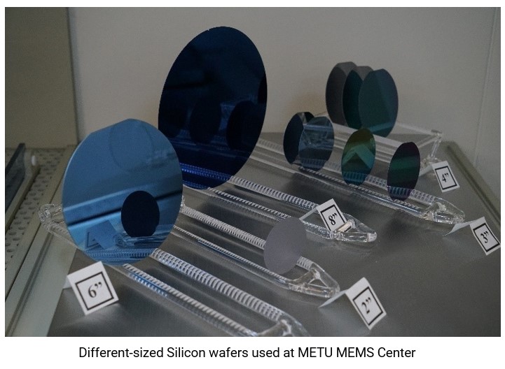
The journey of MEMS production at METU MEMS Center began with processing 3-inch diameter wafers. Over time, through continuous improvement and updates, the capabilities expanded to include 4", 6" and 8" diameter wafers. As a result, the utilization of wafers of various sizes has led to a broader range of production possibilities.
Steps carried out through advanced techniques such as film coating and lithography are crucial stages in the MEMS manufacturing process. High precision and repeatability are necessary for accurate creation of micro and nano-scale structures and successful production of MEMS devices. The film coating stage is a significant step in MEMS manufacturing. In this phase, insulating, conducting, or semiconducting materials with desired electrical and mechanical properties are deposited onto surfaces at specified thicknesses. METU MEMS Center possesses various capabilities in thin film coatings. Some capabilities that METU MEMS Center offers in the realm of thin film coatings include:
- Thin Film Coating Technologies:
At METU MEMS Center, various materials can be coated using different thin film deposition methods. Among these methods are techniques such as Physical Vapor Deposition (PVD), Chemical Vapor Deposition (CVD), and Atomic Layer Deposition (ALD).
- Material Selection:
METU MEMS Center has the capability to perform thin film coatings of various materials suitable for different applications. For instance, metallic coatings (gold, silver, copper), semiconductor coatings (silicon), insulating coatings (oxides, nitrides), and other specialized coatings can be applied.
- Quality Control:
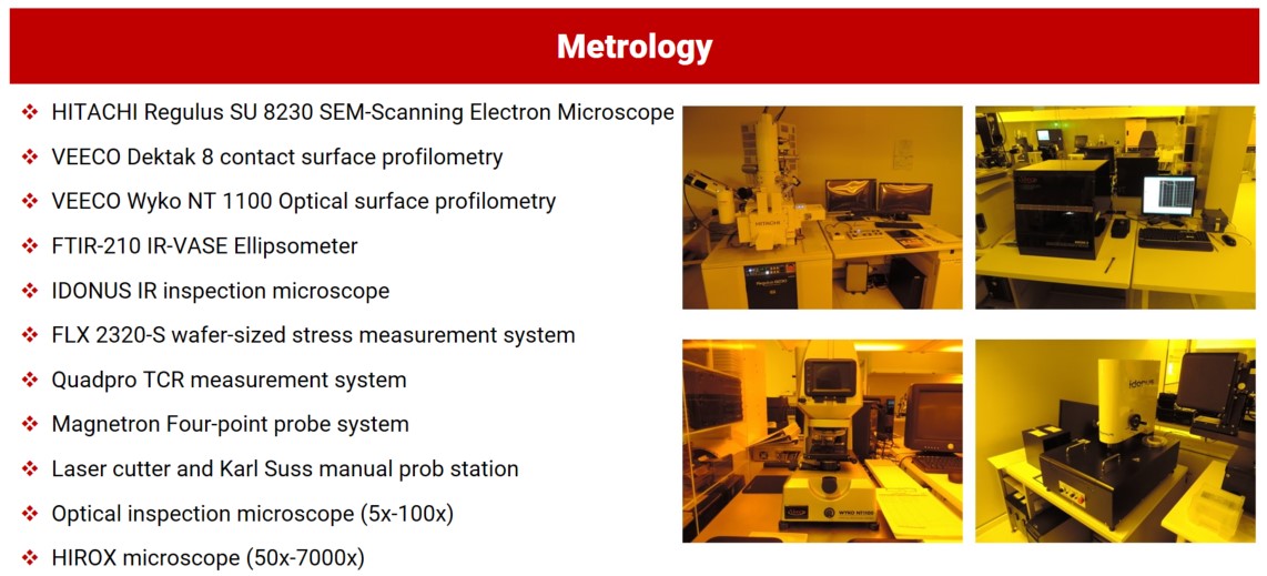
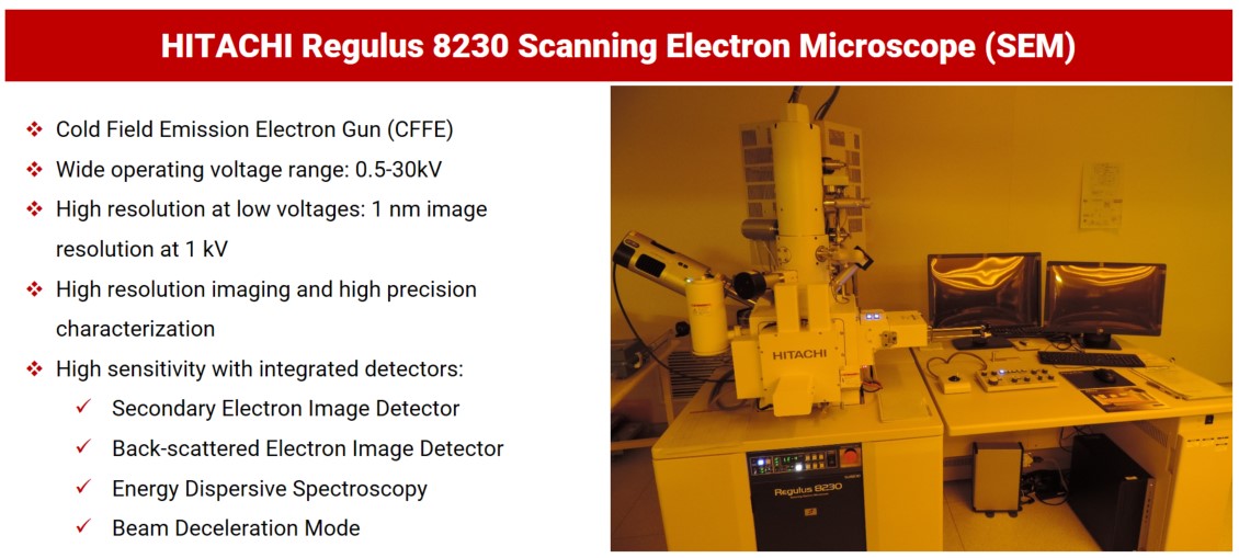
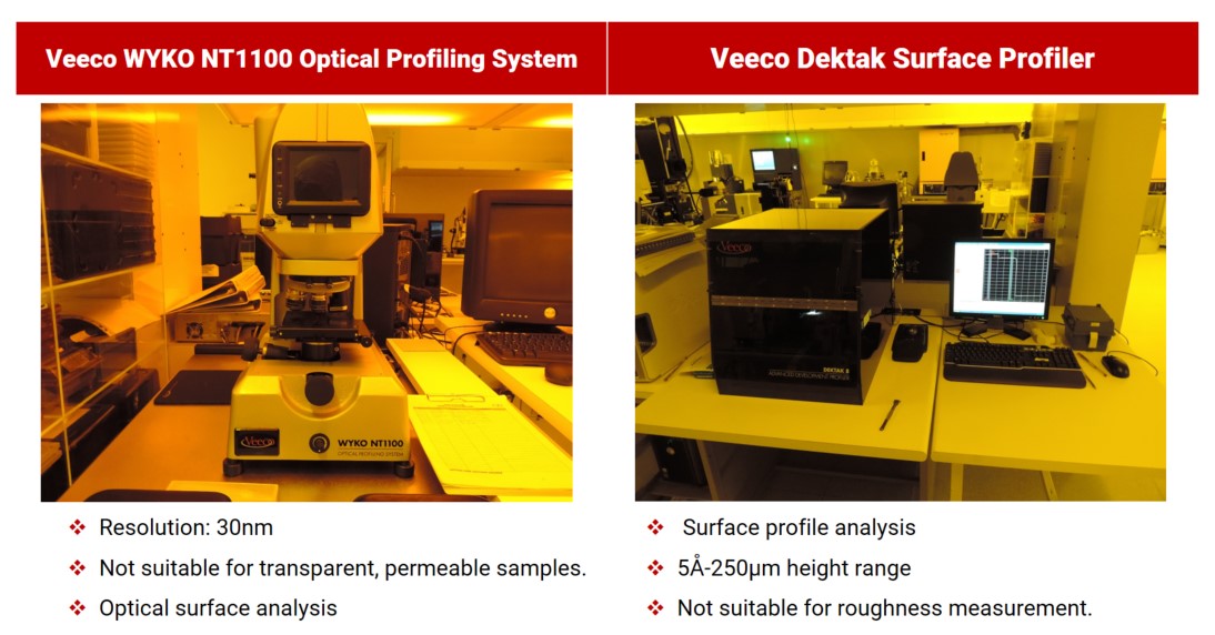
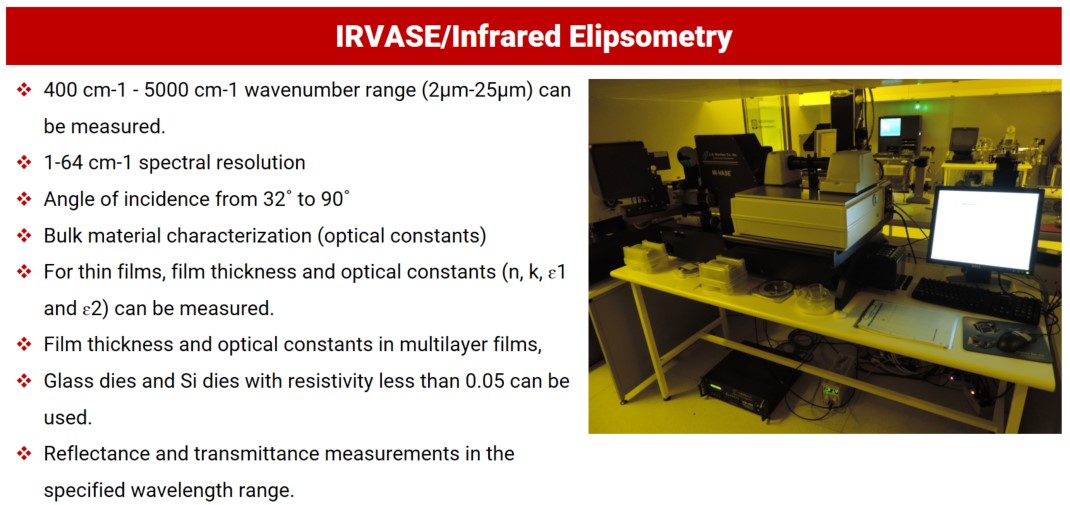
METU MEMS Center possesses various analysis methods to assess the quality of thin film coatings. These methods include surface profilometry, scanning electron microscopy (SEM), energy dispersive spectroscopy (EDS), and IR/VASE ellipsometry.
- Coating Thickness and Uniformity:
METU MEMS Center employs process control to ensure the desired thickness and uniformity of thin film coatings. This enables the production of thin film coatings according to varying thickness requirements.
- Application-Specific Coatings:
METU MEMS Center has the capability to optimize thin film coatings for specific applications. In this context, optical coatings, electromechanical coatings, protective coatings, and other specialized coatings can be implemented.
These capabilities reflect METU MEMS Center's extensive range of services in the field of thin film coatings.
METU MEMS Center possesses various capabilities and equipment in the field of photolithography. Lithography is a fundamental step in microfabrication processes and involves patterning thin films. The lithography capabilities that METU MEMS Center can offer include:
- Mask Design:
METU MEMS Center has expertise in mask design and applications. A mask is a glass containing a specific pattern, shape, or pattern sequence, which is transferred onto a thin film processed using reflected or transmitted light.
- Process Equipment:
METU MEMS Center possesses various equipment used in the lithography process. These include a mask writer used to create masks, coating equipment for applying the photoresist layer, and mask alignment systems for the exposure process.
- Process Parameter Optimization:
METU MEMS Center has the capability to optimize the necessary process parameters for successful lithography. Adjusting parameters such as light source, exposure time, exposure intensity, and development time ensures the accurate transfer of the desired pattern.
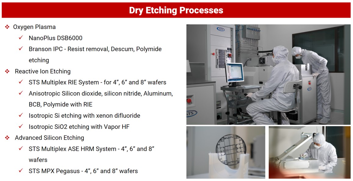
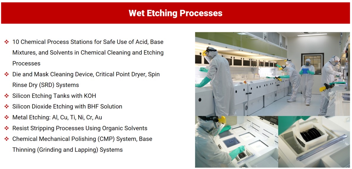
METU MEMS Center possesses the capability for high precision and controlled material processing using methods such as dry and wet etching. Utilizing advanced equipment and experienced experts in dry and wet etching processes enables the accomplishment of high-quality operations. As a result, it becomes possible to optimize the characteristics of various materials, enhance device performance, and achieve desired outcomes.
- Dry Etching:
Dry etching is a process of material erosion using various gases or plasma. METU MEMS Center employs these dry etching methods to achieve the desired size reduction of various materials. These processes involve the use of plasma systems such as Reactive Ion Etching (RIE) and Vapor HF (Hydrofluoric Acid).
- Wet Etching:
Wet etching is the process of material erosion using chemical solutions. METU MEMS Center utilizes the wet etching method for processes such as shaping and flattening materials.
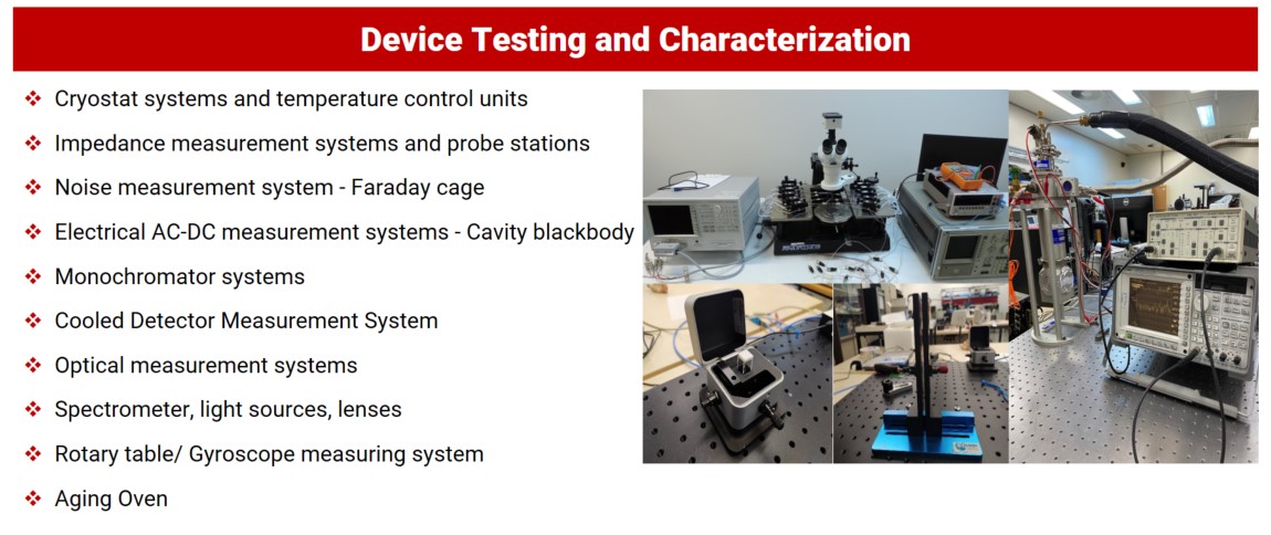
Test and characterization involve various methods used to evaluate, measure, and analyze the performance of MEMS devices.
- Electrical Characterization:
MEMS devices' electrical properties are characterized using methods like current-voltage (IV) measurements, resistance measurements, and capacitance measurements. These tests are conducted to evaluate the devices' electrical performance, operational range, power consumption, and signal processing capabilities.
- Mechanical Characterization:
MEMS devices' mechanical properties are characterized with parameters such as deformation, vibration, and elasticity. These tests are used to assess the devices' durability, vibration tolerance, amount of deformation, and structural integrity.
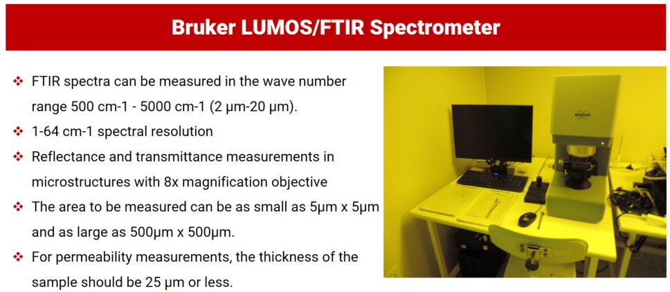
- Optical Characterization:
MEMS devices' optical properties are characterized using parameters like light propagation, reflection, absorption, and light transmittance. These tests are employed to evaluate the devices' optical performance, light processing capabilities, and detection sensitivity.
- Thermal Characterization:
MEMS devices' thermal properties are characterized with parameters like temperature distribution and thermal conductivity. These tests are performed to assess the devices' thermal management and temperature stability capabilities.
- Sensitivity and Accuracy Testing:
The sensitivity, measurement accuracy, and repeatability of MEMS devices are tested. These tests are used to evaluate measurement errors, response times, and reliability of the device.
METU MEMS Center is equipped with the necessary equipment and expert personnel to conduct these and other testing and characterization processes. This enables an objective evaluation of the performance and quality of MEMS devices.
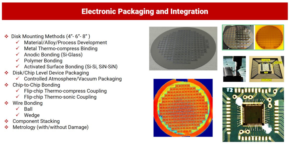
METU MEMS Center possesses the necessary equipment and technical expertise in the field of packaging. The Center is equipped with advanced devices and expert personnel for testing, packaging, and implementing test processes. This ensures the reliable and high-quality packaging of MEMS devices, achieving the desired performance levels.
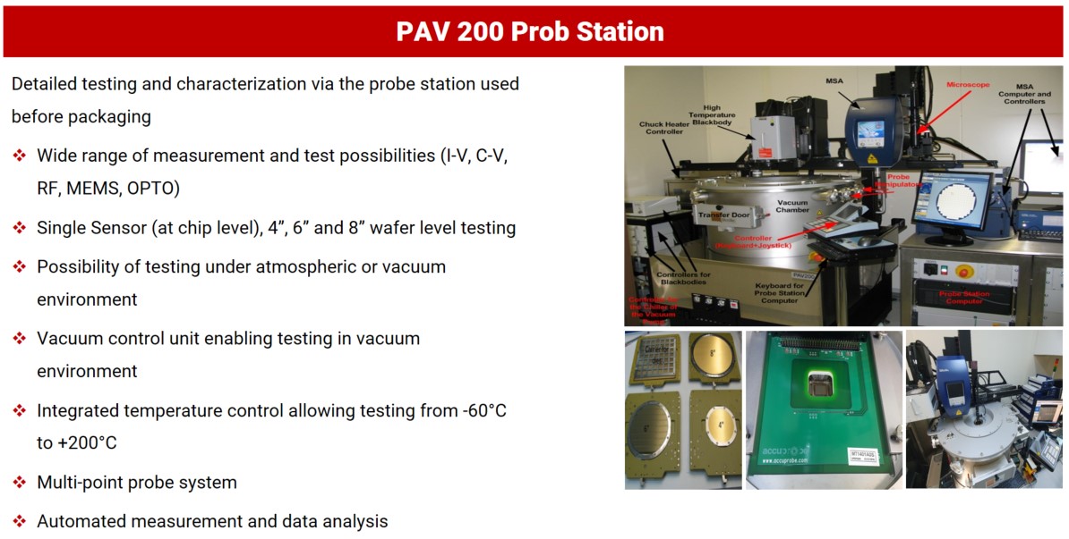
- Test and Cutting Process:
Through probe testing, functioning chips are identified and recorded. Subsequently, the chips proceed to the cutting stage where they are delicately separated. Chips that pass the probe test move on to the packaging stage for placement within the packaging structure.
- Packaging Process:
Packaging is a crucial process that involves testing MEMS devices and placing them within a protective package. The electrical connections of the device placed in the package are established using wire bonding.
- Post-Packaging:
Devices undergo electrical, optical, and mechanical tests to determine if they meet the desired performance levels. The reliability and functionality of the devices are assessed through these tests. Quality control is conducted on packaged devices, and corrections are made if necessary.
The packaging stage ensures the protection of manufactured MEMS devices, establishes their electrical connections, and tests their performance. Packaging devices for readiness prepares them for use, completes the production process, and makes the final products ready for distribution or use.
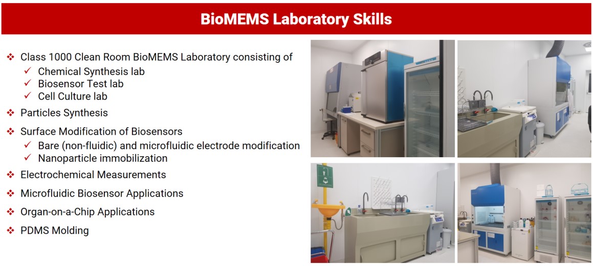
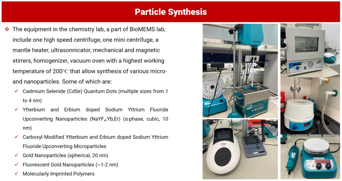
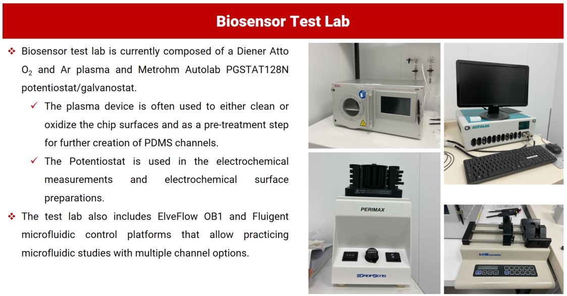
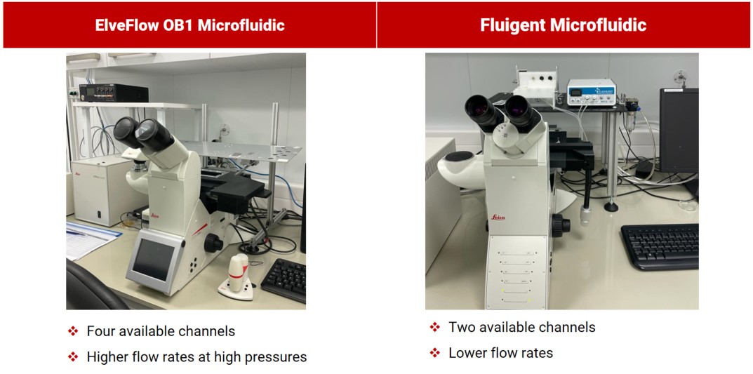
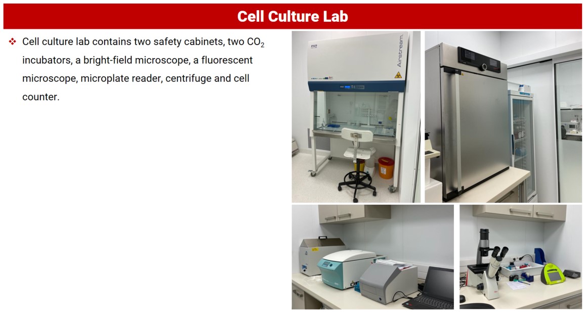
BioMEMS Chemistry and Cell Culture Laboratories were established to conduct various studies in the fields of biology, chemistry, micro and nanotechnology and nanomedicine. The equipment in the cell culture laboratory allows researchers to culture, store, characterize and display any cell type they want. In the chemistry laboratory, polymers, micro and nanoparticles, can be synthesized, chip surfaces can be modified, adsorption-desorption studies can be conducted, electrochemical experiments can be carried out and microfluidic setups can be tested. In gerenal, proof-of-concept studies can be performed within this lab. The devices in the laboratory offer the opportunity for new biosensor designs for cancer, various diseases, molecule or ion determination. All these resources installed in both laboratories are quite sufficient to develop new approaches in the field of nanobiosensor technologies.
BioMEMS Lab Coordinator:
Meltem OKAN AYDIN (M.Sc.)
Contact: maydin![]() mems.metu.edu.tr; +90 312 210 6376
mems.metu.edu.tr; +90 312 210 6376
Detailed Device List
|
|
|
|
|
|
|
|
|
|
|
|
|
|
|
|
|
|
|
|
|
|
|
|
|
|
|
|
|
|
|
|
|
|