Cleanroom Capabilities
Last Updated:
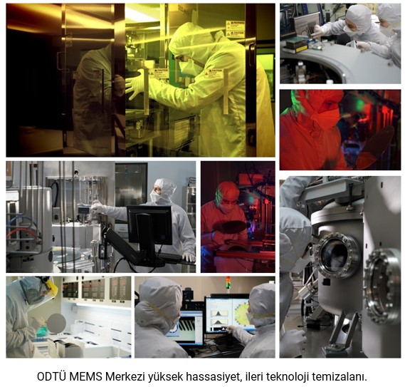
Merkez; toplam 4500 m2'lik kapalı alanda 100, 1.000 ve 10.000 sınıfında çeşitli temiz alan ile laboratuvar, seminer, toplantı ve ofis alanlarına sahip bir tesis olarak faaliyet göstermektedir. Merkez'in bulunduğu ve ODTÜ Teknokent tarafından yönetilmekte olan arazi, ODTÜ Teknokent MET yerleşkesi bünyesinde olup, Sanayi ve Teknoloji Bakanlığı tarafından onaylanan Teknoloji Geliştirme Bölgesi statüsüne sahiptir. Merkez ve Teknokent şirketleri bu yerleşke içinde yer almaktadır. ODTÜ MEMS Merkezi'nde MEMS fabrikasyonunun gerçekleştirilmesine yönelik olarak 1.300 m2'lik bir temizalan bulunmaktadır.
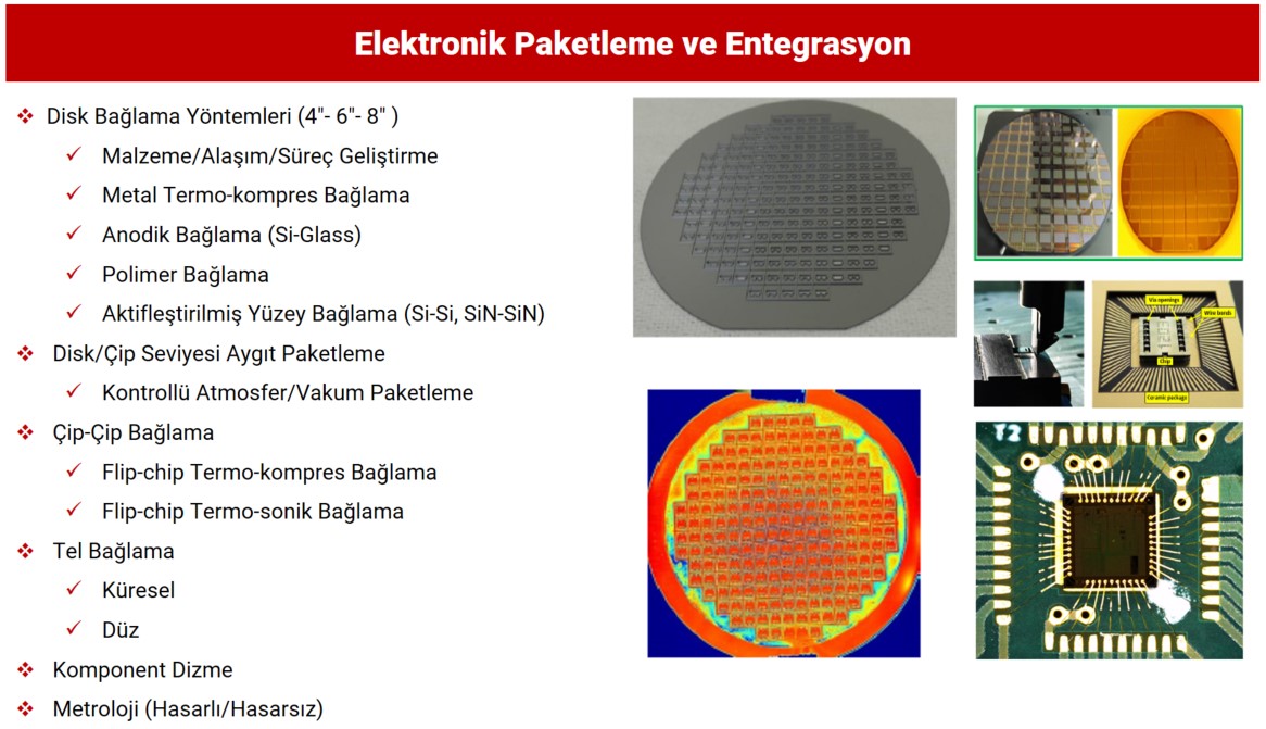
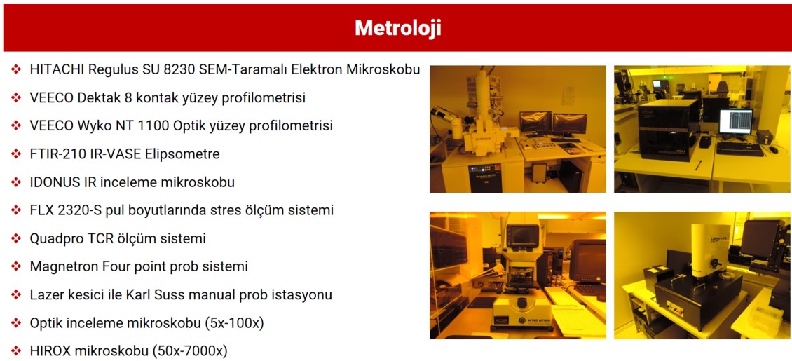
MEMS üretim süreçleri yapılan işlemin niteliğine göre gruplandırılabilmektedir. Bu gruplar; Kaplama, Yüksek Sıcaklık Oksitleme ve Difüzyon, Plazma Ortamında Kuru Kaplama ve Aşındırma, Litografi, Kimyasal Sıvı Aşındırma ve Temizleme, Ölçüm, İnceleme & Test, Elektronik Paketleme ve Entegrasyondur.
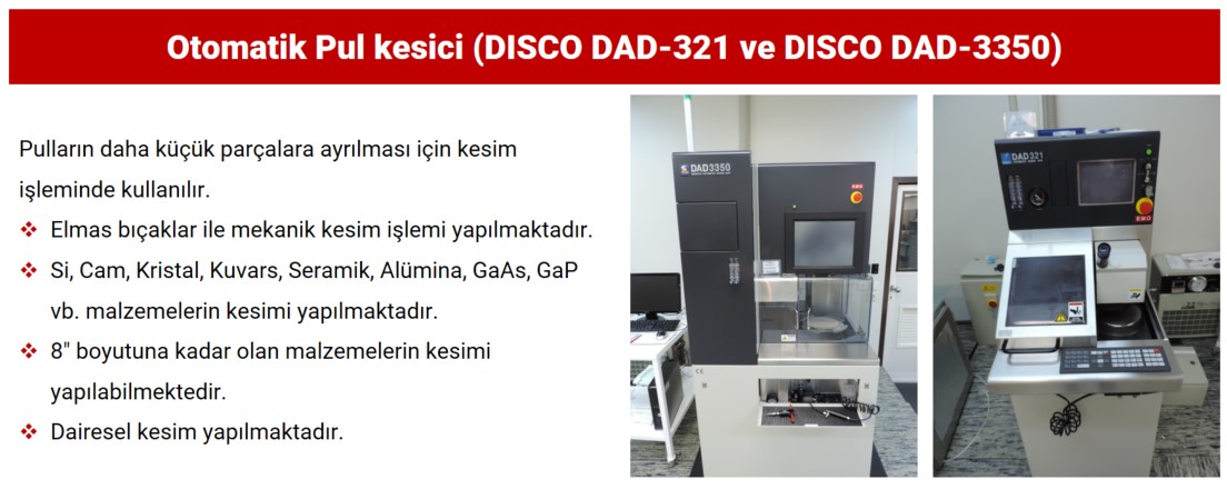
ODTÜ MEMS Merkezi, MEMS üretimine 3" çapındaki pulların işlenmesiyle başlamıştır. Zamanla yapılan iyileştirme ve güncelleştirme faaliyetleri sayesinde 4", 6" ve 8" çapındaki pulların da işlenebilmesi sağlanmıştır. Bu şekilde, farklı boyutlardaki pulların kullanılmasıyla daha geniş bir üretim yelpazesi elde edilmiştir.
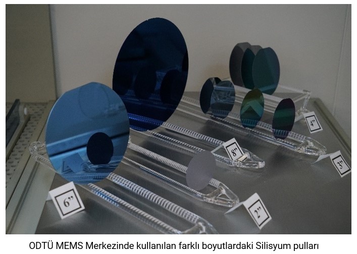
ODTÜ MEMS Merkezinde kullanılan farklı boyutlardaki Silisyum pulları
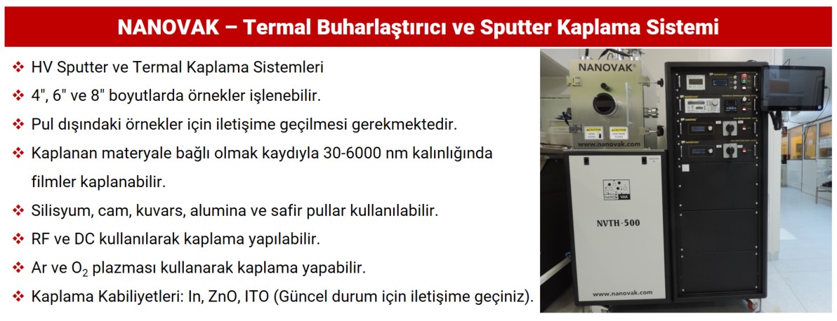
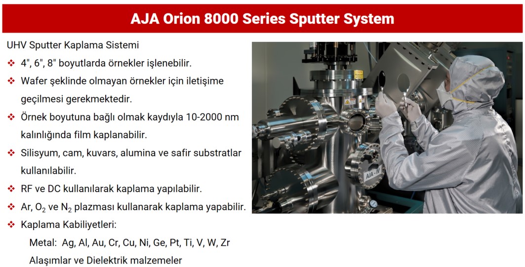
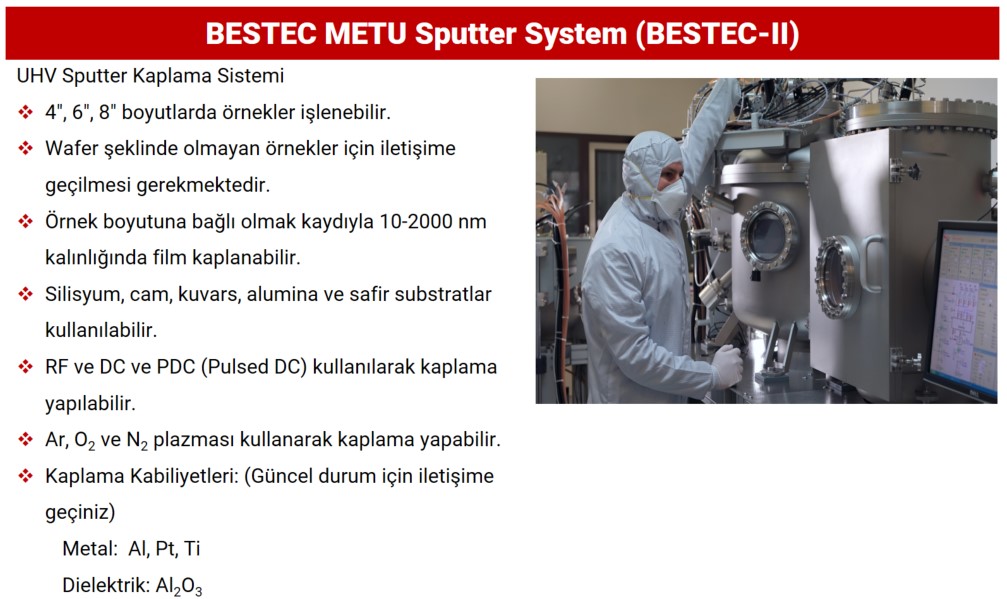
- İnce Film Kaplama Teknolojileri: ODTÜ MEMS Merkezinde farklı ince film kaplama yöntemlerini kullanarak çeşitli malzemeler kaplanabilir. Bu yöntemler arasında fiziksel buhar biriktirme (PVD), kimyasal buhar biriktirme (CVD) ve atomik tabaka biriktirme (ALD) gibi teknikler bulunur.
- Malzeme Seçimi: ODTÜ MEMS Merkezi, farklı uygulamalara uygun olarak çeşitli malzemelerin ince film kaplamalarını gerçekleştirme yeteneğine sahiptir. Örneğin, metalik kaplamalar (altın, gümüş, bakır), yarıiletken kaplamalar (silikon), yalıtkan kaplamalar (oksitler, nitritler) ve diğer özel kaplamalar yapılabilmektedir.
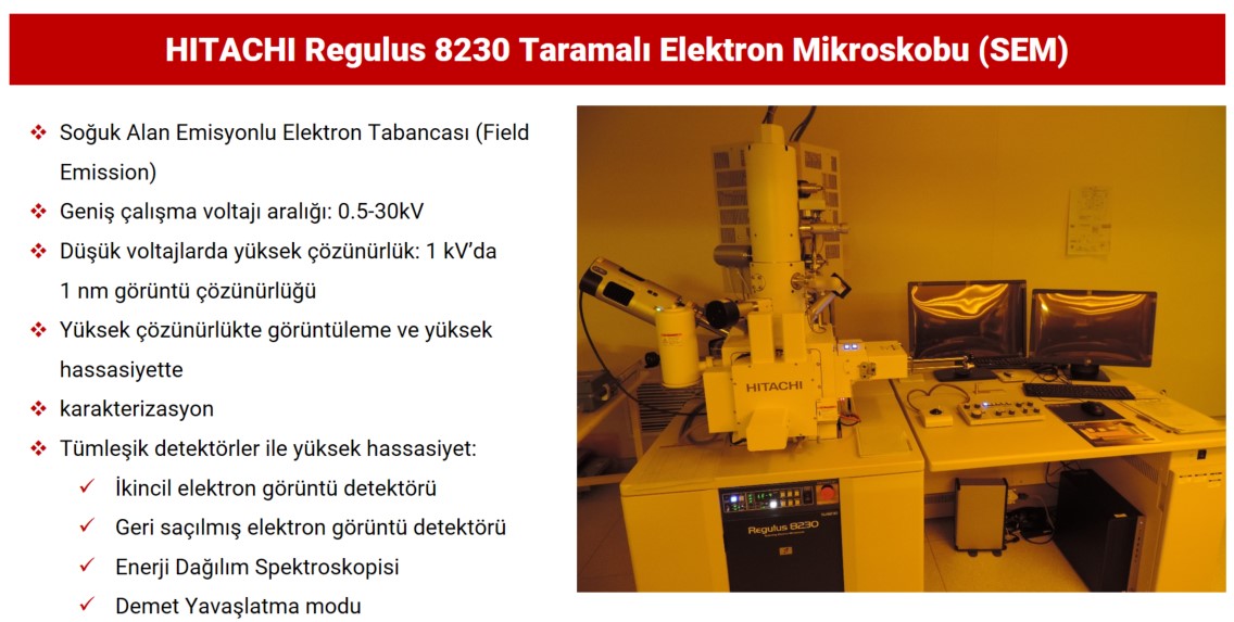
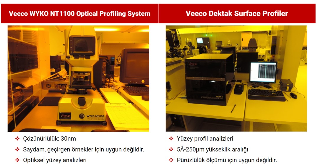
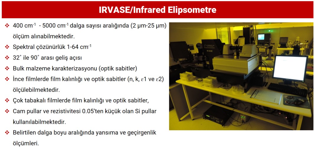
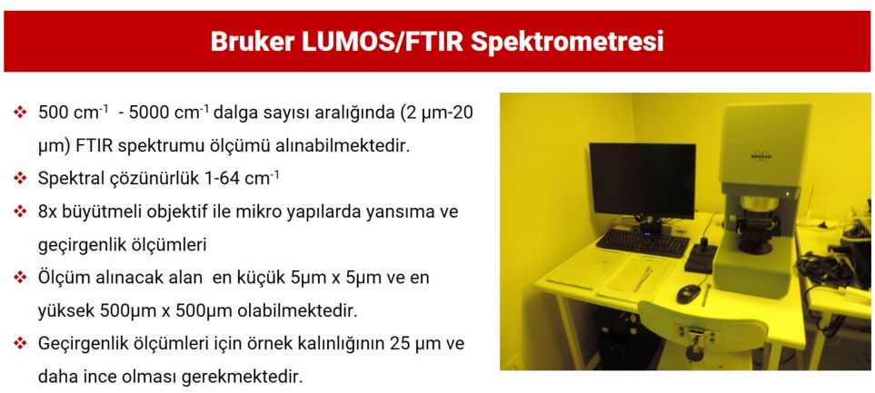
- Kalite Kontrolü: ODTÜ MEMS Merkezi, ince film kaplamalarının kalitesini değerlendirmek için çeşitli analiz yöntemlerine sahiptir. Bu yöntemler arasında yüzey profilometrisi, taramalı elektron mikroskobu (SEM), enerji dağılım spektroskopisi (EDS) ve IR/VASE Elipsometre gibi teknikler bulunur.
- Kaplama Kalınlığı ve Homojenliği: ODTÜ MEMS Merkezi, ince film kaplamalarının istenen kalınlık ve homojenliğe ulaşmasını sağlayacak proses kontrolüne sahiptir. Bu sayede, farklı kalınlık gereksinimlerine uygun olarak ince film kaplamaları üretilebilir.
- Uygulama Odaklı Kaplamalar: ODTÜ MEMS Merkezi, ince film kaplamalarını belirli uygulamalara yönelik olarak optimize edebilme kabiliyetine sahiptir. Bu kapsamda, optik kaplamalar, elektromekanik kaplamalar, koruyucu kaplamalar ve diğer özel uygulamalara yönelik kaplamalar gerçekleştirilebilir.
Bu kabiliyetler, ODTÜ MEMS Merkezi'nin ince film kaplamaları konusunda geniş bir yelpazede hizmet sunma yeteneğini yansıtmaktadır.
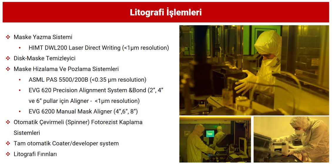
- Maske Tasarımı: ODTÜ MEMS Merkezi, maske tasarımı ve uygulamaları konusunda uzmanlığa sahiptir. Maske, belirli bir deseni, şekli veya desen dizisini içeren camdır ve bu desen, üzerine yansıtılan veya iletilebilen bir ışık kullanılarak işlenen ince film üzerine aktarılır.
- İşlem Ekipmanları: ODTÜ MEMS Merkezi, litografi sürecinde kullanılan çeşitli ekipmanlara sahiptir. Bunlar arasında maskelerin üretildiği maske yazıcı, fotorezist tabakasının kaplandığı kaplama ve pozlama işleminin gerçekleştirildiği maske hizalama sistemleri yer alır.
- İşlem Parametreleri Optimizasyonu: ODTÜ MEMS Merkezi, litografi işleminin başarılı bir şekilde gerçekleştirilmesi için gerekli olan işlem parametrelerini optimize edebilme kabiliyetine sahiptir. Işık kaynağı, pozlama süresi, pozlama yoğunluğu ve geliştirme süresi gibi parametrelerin ayarlanması, istenen desenin doğru bir şekilde aktarılmasını sağlar.
ODTÜ MEMS Merkezi, kuru ve ıslak aşındırma gibi yöntemleri kullanarak yüksek hassasiyet ve kontrollü malzeme işleme yeteneğine sahiptir. Kuru ve ıslak aşındırma işlemlerinde gelişmiş ekipmanlar ve deneyimli uzmanlar kullanarak yüksek kalitede işlemler gerçekleştirebilir. Bu sayede, çeşitli malzemelerin özelliklerini optimize etmek, aygıtların performansını artırmak ve istenen sonuçları elde etmek mümkün olur.
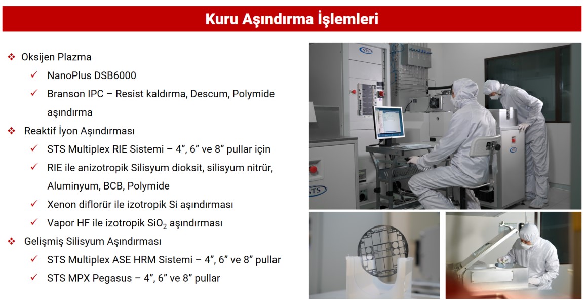
- Kuru Aşındırma: Kuru aşındırma, malzemenin yüzeyini çeşitli gazlar veya plazma kullanarak aşındırma işlemidir. ODTÜ MEMS Merkezi, bu kuru aşındırma yöntemlerini kullanarak çeşitli malzemelerin istenilen boyutlarda aşındırılmasını sağlamaktadır. Bu süreçler, RIE (Reactive Ion Etching) ve Vapor HF (Hydrofluoric Acid) gibi plazma sistemlerinin kullanımını içerir.
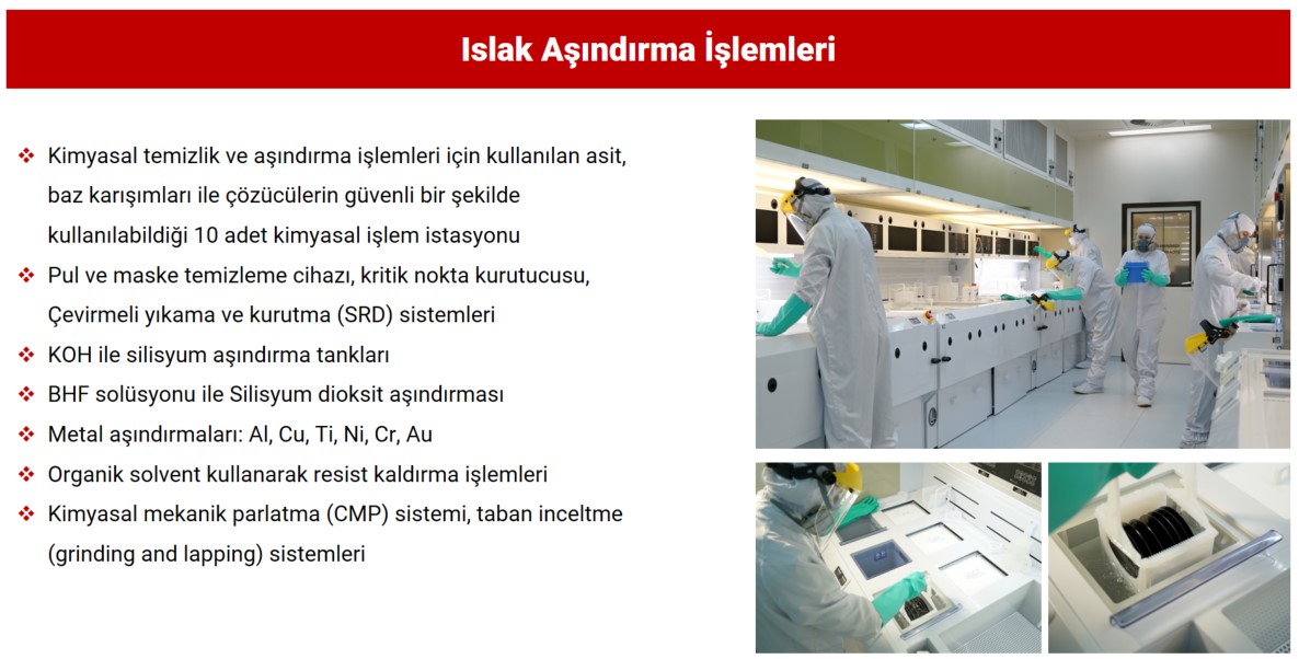
- Islak Aşındırma: Islak aşındırma, malzemelerin kimyasal çözeltiler kullanılarak aşındırılması işlemidir. ODTÜ MEMS Merkezi, ıslak aşındırma yöntemini kullanarak malzemelerin şekillendirilmesi ve düzleştirilmesi gibi işlemleri gerçekleştirir.
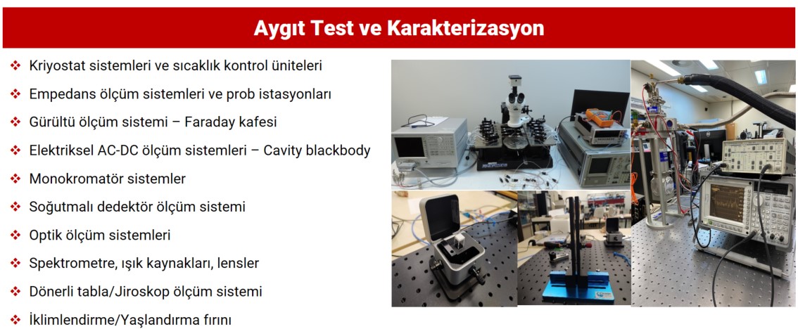
- Elektriksel Karakterizasyon: MEMS aygıtlarının elektriksel özellikleri, akım-voltaj (IV) ölçümleri, direnç ölçümleri, kapasite ölçümleri gibi yöntemlerle karakterize edilir. Bu testler, aygıtların elektriksel performansını, çalışma aralığını, güç tüketimini ve sinyal işleme yeteneklerini değerlendirmek için yapılır.
- Mekanik Karakterizasyon: MEMS aygıtlarının mekanik özellikleri, deformasyon, titreşim, elastiklik gibi parametrelerle karakterize edilir. Bu testler, aygıtların dayanıklılığını, titreşim toleransını, deformasyon miktarını ve yapısal bütünlüğünü değerlendirmek için kullanılır.
- Optik Karakterizasyon: MEMS aygıtlarının optik özellikleri, ışık yayılması, yansıma, soğurma, ışık geçirgenliği gibi parametrelerle karakterize edilir. Bu testler, aygıtların optik performansını, ışık işleme yeteneklerini ve algılama hassasiyetini değerlendirmek için kullanılır.
- Termal Karakterizasyon: MEMS aygıtlarının termal özellikleri, sıcaklık dağılımı ve termal iletkenlik gibi parametrelerle karakterize edilir. Bu testler, aygıtların termal yönetimini ve sıcaklık sabiti gibi yeteneklerini değerlendirmek için yapılır.
- Hassasiyet ve Doğruluk Testleri: MEMS aygıtlarının hassasiyeti, ölçüm doğruluğu ve tekrarlanabilirlik gibi parametrelerle test edilir. Bu testler, aygıtların ölçüm hatasını, yanıt süresini ve güvenilirliğini değerlendirmek için kullanılır.
ODTÜ MEMS Merkezi, bu ve diğer test karakterizasyonlarını yapabilmek için gerekli ekipmanlara ve uzman personellere sahiptir. Bu sayede MEMS aygıtlarının performansını ve kalitesini objektif bir şekilde değerlendirmek mümkün olur.
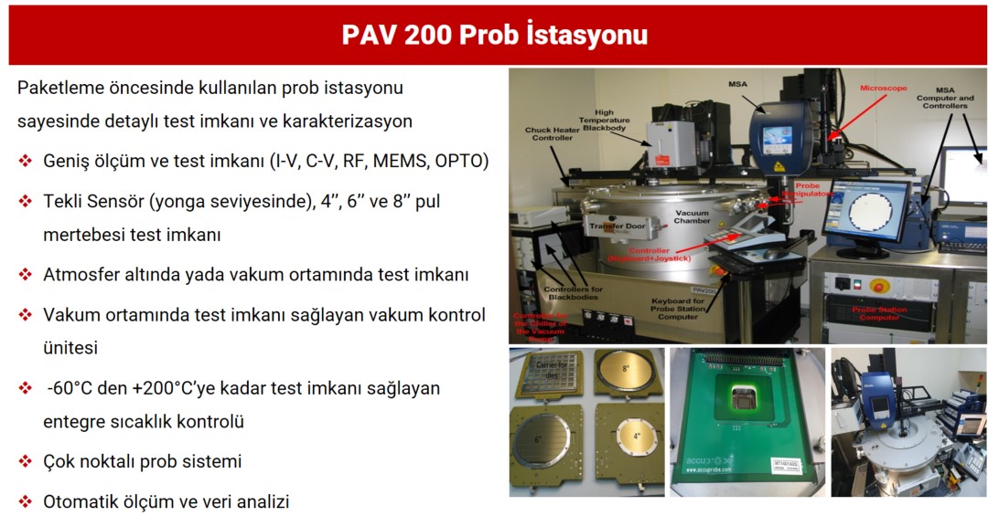
- Test ve kesim işlemi: Prob testi ile, çalışan çipler tespit edilir ve kaydedilir. Ardından çipler kesim aşamasına geçer ve hassas bir şekilde kesilip birbirinden ayrılır. Prob testi aşamasından geçen çipler, paket yapısına yerleştirilmek üzere paketleme aşamasına ilerler.
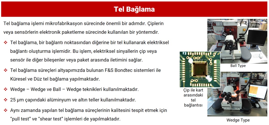
- Paketleme işlemi: MEMS aygıtlarının test edilmesi ve koruyucu bir paket içerisine yerleştirilmesini içeren önemli bir süreçtir. Pakete yerleştirilen aygıtın elektriksel bağlantılarının yapılması için tel bağlama yöntemi kullanılarak gerçekleştirilir.
- Paketleme sonrası: Elektriksel, optik ve mekanik testlere tabi tutulur. Bu testler, aygıtların istenen performans seviyelerini sağlayıp sağlamadığını belirlemek için yapılır. Aygıtların güvenilirliği ve işlevselliği bu testlerle değerlendirilir. Bu aşamada, paketlenen aygıtların kalite kontrolü sağlanır ve gerektiğinde düzeltmeler yapılır.
Paketleme aşaması, üretilen MEMS aygıtlarının korunmasını, elektriksel bağlantılarının sağlanmasını ve performanslarının test edilmesini sağlar. Aygıtların paketlenerek kullanıma hazır hale getirilmesi, üretim sürecinin tamamlanmasını ve son ürünlerin dağıtıma veya kullanıma sunulmasını sağlar.