
AYGIT PAKETLEME
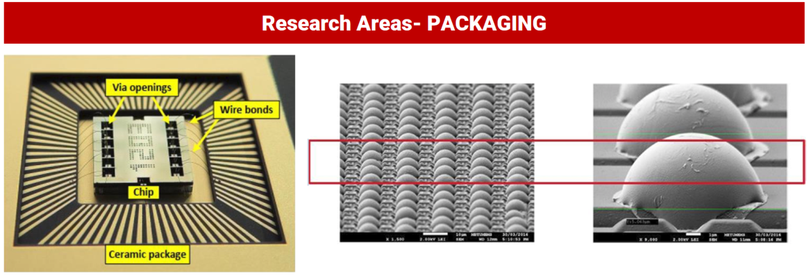
The research area of packaging, representing the final step in the transformation of MEMS-based devices into products, includes the definition and development of packaging, microfabrication, and testing processes.
The package structure serves as the interface, providing mechanical, electronic, and optical connections between the MEMS-based chip and the systems into which they will be integrated. Additionally, the package structure can accommodate integrated circuits and establish the necessary interfaces between these chips and devices. One of the key factors influencing the pricing of MEMS products is the packaging process. With the projects and studies carried out in the past within the scope of this field, a significant amount of experience and knowledge has been gained regarding the packaging of MEMS devices. Today, ongoing research aims to develop low-cost packaging technologies using innovative approaches.